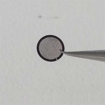
투과 전자 현미경(Transmission Electron Microscope, TEM) 측정을 위해 TEM Grid위에 TCVD Graphene on Cu foil 의 monolayer 그래핀을 transfer 하여 드립니다.
PMMA 0%를 원하시는 분은 따로 메모 남겨주세요!
Properties of Graphene on TEM Grid
| Grid Hole Size : 63 μm | Sheet Resistance : Av.< 250~400 Ω/sq |
| Lacey Carbon Type-A | Mobility : >3500 ㎠/Vs (Max. 17,000 ㎠/Vs |
| 300 mesh | Transmittance : >97% |
| Copper Frame | Coverage : <30% (PMMA-free), <60% (2-layers) |
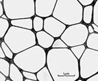
Lacey Carbon Type-A
A Lacey carbon film with a removable Formvar backing on the opposite side of the grid. When the Formvar is removed, by dipping in solvent, the Lacey carbon film remains. These films are stable under all EM(electron microscopy) operating conditions and for use where the presence of Formvar can not be tolerated. Pure Lacey Carbon is more delicate than those with Formvar backing and require more careful handling during specimen preparation. Holes are completely open.
Lacey Support Film
Bare TEM Grid
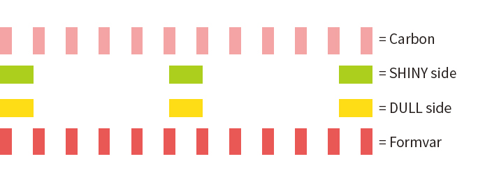
Support Film Product Note, How the Material is Layered on the Grid
Most of the grids used have a distinct “shiny” side and “dull” side when viewed with the naked eye. Generally, the film type as specified in the product name lies on the shiny side of the grid.
Lacey carbon Type A
The Lacey formvar film is applied to the dull side of the grid and carbon depositied onto the shiny side. When the formvar is removed in solvent the carbon film is left on the shiny side.
Grid Cross Section
| Substrate Application | Carbon Type-A | Is Lacey Film suitable for this application? |
|---|---|---|
| Applications Requiring Pure Formvar | Not Suitable | No |
| Bacterial Suspensions | Best | Yes |
| Cell Fragment Suspensions | Best | Yes |
| Diffraction Studies | Best | Yes |
| EDS (energy dispersive spectrometry) | Best | Yes |
| High Resolution Microscopy | Best | Yes |
| High Temperature Techniques / Heating Stage | Best | Yes(Type-A) |
| Low Magnification Microscopy | Good Alternative | No |
| Particulate Suspension, Biological | Best | Yes |
| Particulate Suspension, Non-Biological | Best | Yes |
| Powders, Dry | Good Alternative | No |
| Replicas & Low Temperature Techniques | Good Alternative | Yes(Type-A) |
| Thin Sections | Good Alternative | Yes |
| Viral Suspensions | Best | Yes |
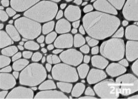
Measurement data
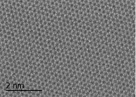
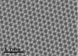
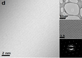
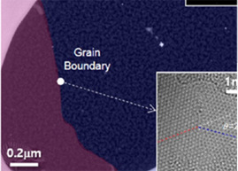
(d) HR-TEM results showing the atomic lattice structures of RT-CVD graphene. The graphene samples were prepared with holey carbon grid (upper inset). The aberration-corrected scanning TEM image provides an atom-by-atom analysis of graphene (mid inset). The diffraction pattern indicates the corresponding graphene is a highly crystalline monolayer (lower inset). (e) Graphene domain distribution investigated by selected area diffraction patterns (SADP) and TEM imaging. (f) Graphene boundaries of RT-CVD graphene characterized by dark-field TEM and aberration-corrected HR-TEM images . The left and right parts of the grain boundary are imaged with an aperture at the red and blue circled spots of the diffraction pattern (upper inset). The atomic image shows that two graphene domains are smoothly connected with an angle of 36° (lower inset). See also Supporting Figure S2 for more dark-field TEM analyses.
Spot 1 (top)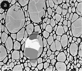
Spot 2 (center)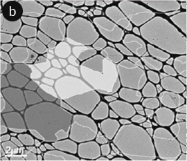
Spot 3 (bottom)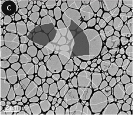
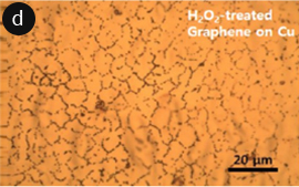
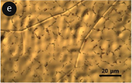
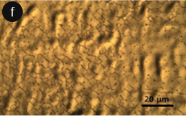
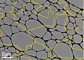
Figure 4. Grain boundary analyses by TEM and OM. (a-c) Grain boundary mapping of RT-CVD graphene films by TEM corresponding to the sheet resistance of spots 1, 2, and 3 in Figure 3a, respectively. (d-f) Grain boundary mapping of H2O2-treated RT-CVD graphene on Cu foils by optical microscopes, corresponding to the red spots 1, 2, and 3 in Figure 3a, respectively. The grain size of graphene in the center region is a few times larger than the edge region. But actually, there is no significant difference in sheet resistance (226, 227, and 230 Ω/sq for spots 1, 2, and 3, respectively).
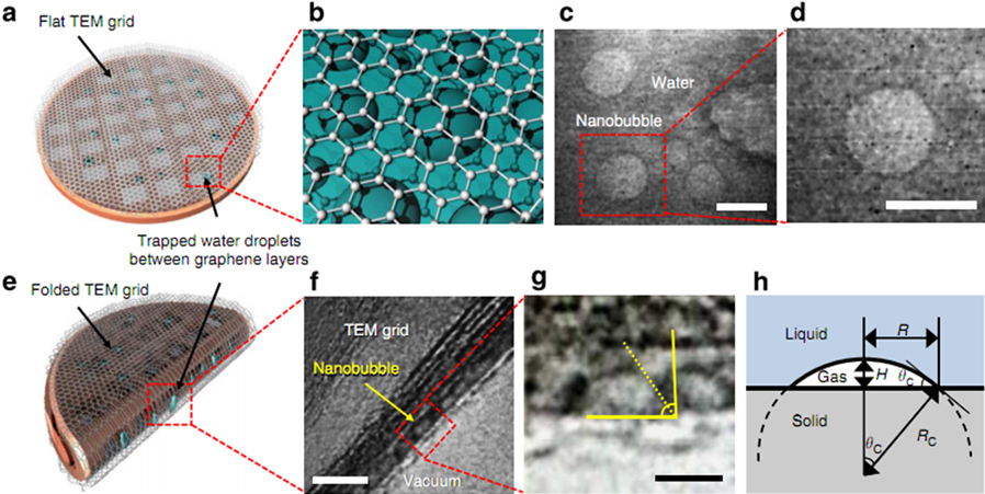
Figure 1 | Morphology of nanobubbles in graphene liquid cell. (a?d) A graphene liquid cell fabricated on a ?at TEM grid (copper or molybdenum) showing the top views of nanobubbles. (c and d) In-situ snapshot images of nanobubbles obtained by ultra-high vacuum (UHV) TEM (200 keV, ~5X10⁻⁹ Torr). Scale bars, 10 nm. (e?g) A folded graphene liquid cell showing the side views of nanobubbles. The contact angles were roughly measured to be 6o°?90°. Scale bars for f and g, 10 and 5 nm, respectively.
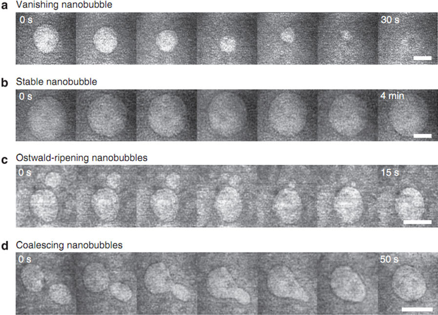
Figure 2 l Time evolution of different kinds of single and double nanobubbles. (a,b) The snap shots of Tem images showing the vanishing and stable nanobubbles, respectively. The nanobubbles smaller than critical radius tend to shrink with time and disappear in ~40s, whereas the larger bubbles persist for more than 10 min. Scale bar, 5 nm. The full movie is available in Supplementary Movie 2. (c,d) The snap shots of TEM images showing the merging of adjacent two nanobubbles observed for 15 and 50 s, respectively. When the nanobubble sizes are significantly different, it show an Ostwald ripening-like merging process, whereas the similar-sized bubbles are coalescing as their inter-bubble boundary breaks. Scale bar, 10nm. The full movie is available in Supplementary Movie 3.
Reference
(1) Ryu, Jaechul, et al. "Fast synthesis of high-performance graphene films by hydrogen-free rapid thermal chemical vapor deposition.” ACS nano 8.1 (2014): 950-956.
(2) Park, Jooyeon, et al. “Graphene?Regulated Cardiomyogenic Differentiation Process of Mesenchymal Stem Cells by Enhancing the Expression of Extracellular Matrix Proteins and Cell Signaling Molecules.” Advanced healthcare materials 3.2 (2014): 176-181.
(3) Shin, Dongha, et al. “Growth dynamics and gas transport mechanism of nanobubbles in graphene liquid cells." Nature communications 6 (2015).
(4) Kim, Yeonho, et al. "High-performance ultraviolet photodetectors based on solution-grown ZnS nanobelts sandwiched between graphene layers." Scientific reports 5 (2015).
(5) Sim, Uk, et al. "N-doped graphene quantum sheets on silicon nanowire photocathodes for hydrogen production." Energy & Environmental Science 8.4 (2015): 1329-1338.
(6) Moon, Joonhee, et al. "One?Step Synthesis of N?doped Graphene Quantum Sheets from Monolayer Graphene by Nitrogen Plasma." Advanced Materials 26.21 (2014): 3501-3505.
(7) Kim, Sang Jin, et al. "Simultaneous etching and doping by Cu-stabilizing agent for high-performance graphene-based transparent electrodes." Chemistry of Materials 26.7 (2014): 2332-2336.
(8) Kim, Jung Kyu, et al. "Surface-Engineered Graphene Quantum Dots Incorporated into Polymer Layers for High Performance Organic Photovoltaics." Scientific reports 5 (2015).
Nature Nanotechnology 2010 cover image.
최적화된 연구 환경에서 진행됩니다. Less residue, clear surface, Coverage 95% 이상, 기판 표면 개질 등
질소 충진 진공포장 표면 contact zero Handling이 용이한 packing
옵션/추가공정으로 연구방향에 맞는 그래핀 샘플 advice 그래핀 연구 경험이 없으신 분들, 새로운 기판에 그래핀 적용을 원하시는 분들께 추천합니다.
품질 이상 시, 100% 재제작 언제든 연락주세요.
장비부터 Transfer까지 모든 공정에 대한 이해를 기반으로 오직 그래핀만을 위한 CVD 장비 취급부터 그래핀만을 위한 합성, 전사, 포장 공정.
 02
완충재 포장
03
택배사 픽업
02
완충재 포장
03
택배사 픽업
| 주문 과정 |  고객 주문/결제 고객 주문/결제 |
 그래핀 샘플 제작 그래핀 샘플 제작 |
 포장 포장 |
 배송(우체국 택배 이용) 배송(우체국 택배 이용) |
|---|---|---|---|---|
| 진행 현황 | 고객의 주문을 확인하고 검토합니다 | 고품질 샘플을 제작하고 품질검사를 진행합니다 | 운반과 취급에 대비해 안전하게 포장합니다 | 주문하신 제품을 발송합니다(일반적으로 3영업일이 소요됩니다) |
그래핀 스퀘어의 Transferred Graphene product의 Manufacturing process에 대해 알고 싶습니다.
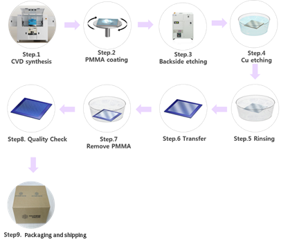
1) Thermal CVD equipment로 graphene synthesis
2) PMMA coating
3) Back side etching (RIE 이용)
4) APS 용액 위에서 Cu foil etching
5) DIW에 rinsing
6) Substrate에 transfer, Drying, Baking(@hot plate)
7) PMMA 제거(Acetone dipping)
8) Quality check (Optical microscope, Raman spectroscope)
9) Vacuum package, shipping
판매하고 있는 크기 외에 다른 사이즈 CVD Graphene on Cu foil도 구매가 가능한가요?
현재 저희가 판매하고 있는 [TCVD Graphene on Cu foil] 제품은 최소 사이즈가 50x50mm 입니다. 해당 제품보다 작은 크기가 필요하시다면 50x50mm를 구매하셔서 cutting 하여 사용하는 것을 추천합니다. 80x80mm보다 큰 제품이 필요하시면 아래 메일로 연락 부탁 드립니다. info@graphenesq.com
그래핀을 처음 다루는데, substrate(SiO2/Si wafer, glass, PET,,,)에 전사된 그래핀을 사용하려고 합니다.
연구원님께서 직접 Graphene on Cu foil을 구매하셔서 직접 transfer 공정을 진행하실 수도 있으나, 숙련되지 않은 상태라면 많은 시행착오를 겪게 되리라 예상됩니다.
위와 같은 위험요소가 부담되신다면, 저희의 transferred graphene을 구매하시거나, transfer service를 이용하시는 것을 추천 드립니다.
< Custom Made Order link 연결>
Stacked graphene은 각층마다 PMMA 코팅을 하여 전사하는 건가요? 아니라면 어떤 방식으로 제작되나요?
2층 이상의 적층 샘플의 경우는 Cu foil에서 성장한 그래핀을 여러층 겹치는 공정으로 제작됩니다.
간략히 적층 방법을 말씀드리면, DIW상의 [PMMA/Graphene]를 [Graphene/Cu foil]로 아래에서 떠서 [PMMA/Graphene/Graphene/Cu foil]을 만듭니다. 이후 또다시 Cu foil etching 및 위 과정을 반복하여 n층의 그래핀 샘플을 제작합니다.
그래핀을 이용하여 사출물과 Press물을 제작 할 수있는지?
그래핀은 아시는 것처럼 graphite(흑연)에서 분리하여 powder 또는 solution 타입으로 얻을 수도 있고(top-down 방식),탄소로 구성된 gas(ex. CH4, C2H4,,,)를 고온에서 합성하여 film 타입으로 얻을 수도 있습니다.(bottom-up 방식, 주로 CVD 합성법 이용)
연구 방향에 따라 위의 두 가지 타입 중 선택하여 사용하는 것이 가능합니다. 그래핀 특성은 이론적인 값과 실제 샘플의 값에서 어느 정도 차이가 있으며, powder인지 film인지에 따라서도 다른 특성을 가지고 있습니다.
그래핀을 다른 물질과 섞어서 쓰시기에는 powder 타입이 더 적합할 것으로 판단됩니다. 비율에 따라 테스트를 해봐야겠지만, 일반적으로 그래핀 powder와 다른 물질을 섞어 사출하는 것은 가능합니다.
Dry transfer로 그래핀 샘플을 만들고 싶습니다. 어떻게 해야 할까요?
1. Dry transfer의 경우는 크게 (1)Thermal release tape와 (2)PSAF(자가점착필름) 방법이 있습니다. 일단, 두 가지 방법 모두 laminator에서 압력을 가해야 한다는 것이 공통점입니다.
간단하게 두가지 방법에 대해 소개를 드리자면 :
1) Thermal release tape: 균일한 압력과 열(100~110℃)을 동시에 가해 지지층 필름(TRT)의 점착력을 잃게 하여 그래핀 전사를 하는 방식입니다. (오랜 기간 노하우가 쌓여서 두 가지 방법 중 더 안정한 방식이라고 말씀드릴 수 있습니다.)
2) PSAF(자가점착필름): 균일한 압력만 가하여 그래핀을 지지필름(자가점착필름)에서 기판으로 그래핀을 전사하는 방식입니다.
그래핀 스퀘어의 Transferred Graphene product의 Manufacturing process에 대해 알고 싶습니다.
1) Thermal CVD equipment로 graphene synthesis
2) PMMA coating
3) Back side etching (RIE 이용)
4) APS 용액 위에서 Cu foil etching
5) DIW에 rinsing
6) Substrate에 transfer, Drying, Baking(@hot plate)
7) PMMA 제거(Acetone dipping)
8) Quality check (Optical microscope, Raman spectroscope)
9) Vacuum package, shipping
판매하고 있는 크기 외에 다른 사이즈 CVD Graphene on Cu foil 도 구매가 가능한가요?
현재 저희가 판매하고 있는 [TCVD Graphene on Cu foil] 제품은 최소 사이즈가 50x50mm입니다. 해당 제품보다 작은 크기가 필요하시다면 50x50mm를 구매하셔서 cutting 하여 사용하는 것을 추천합니다. 80x80mm보다 큰 제품이 필요하시면 아래 메일로 연락 부탁 드립니다. info@graphenesq.com
그래핀 스퀘어의 Transferred Graphene product의 Manufacturing process에 대해 알고 싶습니다.
1) Thermal CVD equipment로 graphene synthesis
2) PMMA coating
3) Back side etching (RIE 이용)
4) APS 용액 위에서 Cu foil etching
5) DIW에 rinsing
6) Substrate에 transfer, Drying, Baking(@hot plate)
7) PMMA 제거(Acetone dipping)
8) Quality check (Optical microscope, Raman spectroscope)
9) Vacuum package, shipping
그래핀을 처음 다루는데, substrate(SiO2/Si wafer, glass, PET,,,)에 전사된 그래핀을 사용하려고 합니다.
연구원님께서 직접 Graphene on Cu foil을 구매하셔서 직접 transfer 공정을 진행하실 수도 있으나, 숙련되지 않은 상태라면 많은 시행착오를 겪게 되리라 예상됩니다.
위와 같은 위험요소가 부담되신다면, 저희의 transferred graphene을 구매하시거나, transfer service를 이용하시는 것을 추천 드립니다.
< Custom Made Order link 연결>
그래핀 스퀘어의 Transferred Graphene product의 Manufacturing process에 대해 알고 싶습니다.
1) Thermal CVD equipment로 graphene synthesis
2) PMMA coating
3) Back side etching (RIE 이용)
4) APS 용액 위에서 Cu foil etching
5) DIW에 rinsing
6) Substrate에 transfer, Drying, Baking(@hot plate)
7) PMMA 제거(Acetone dipping)
8) Quality check (Optical microscope, Raman spectroscope)
9) Vacuum package, shipping
그래핀을 이용하여 사출물과 Press물을 제작 할 수 있는지
그래핀은 아시는 것처럼 graphite(흑연)에서 분리하여 powder 또는 solution 타입으로 얻을 수도 있고(top-down 방식),탄소로 구성된 gas(ex. CH4, C2H4,,,)를 고온에서 합성하여 film 타입으로 얻을 수도 있습니다.(bottom-up 방식, 주로 CVD 합성법 이용)
연구 방향에 따라 위의 두 가지 타입 중 선택하여 사용하는 것이 가능합니다. 그래핀 특성은 이론적인 값과 실제 샘플의 값에서 어느 정도 차이가 있으며, powder인지 film인지에 따라서도 다른 특성을 가지고 있습니다.
그래핀을 다른 물질과 섞어서 쓰시기에는 powder 타입이 더 적합할 것으로 판단됩니다. 비율에 따라 테스트를 해봐야겠지만, 일반적으로 그래핀 powder와 다른 물질을 섞어 사출하는 것은 가능합니다.
그래핀 스퀘어의 Transferred Graphene product의 Manufacturing process에 대해 알고 싶습니다.
1) Thermal CVD equipment로 graphene synthesis
2) PMMA coating
3) Back side etching (RIE 이용)
4) APS 용액 위에서 Cu foil etching
5) DIW에 rinsing
6) Substrate에 transfer, Drying, Baking(@hot plate)
7) PMMA 제거(Acetone dipping)
8) Quality check (Optical microscope, Raman spectroscope)
9) Vacuum package, shipping
Dry transfer로 그래핀 샘플을 만들고 싶습니다. 어떻게 해야 할까요?
Dry transfer의 경우는 크게 (1)Thermal release tape와 (2)PSAF(자가점착필름) 방법이 있습니다. 일단, 두 가지 방법 모두 laminator에서 압력을 가해야 한다는 것이 공통점입니다.
간단하게 두가지 방법에 대해 소개를 드리자면,
1) Thermal Release Tape [TRT], 2) Pressure Sensitive Adhesive Film [PSAF]. The common requirement is that both methods require pressure using a laminator.
(1) Thermal release tape: 균일한 압력과 열(100~110℃)을 동시에 가해 지지층 필름(TRT)의 점착력을 잃게 하여 그래핀 전사를 하는 방식입니다. (오랜 기간 노하우가 쌓여서 두 가지 방법 중 더 안정한 방식이라고 말씀드릴 수 있습니다.)
2) PSAF(자가점착필름): 균일한 압력만 가하여 그래핀을 지지필름(자가점착필름)에서 기판으로 그래핀을 전사하는 방식입니다.
Stacked graphene은 각층마다 PMMA 코팅을 하여 전사하는 건가요? 아니라면 어떤 방식으로 제작되나요?
2층 이상의 적층 샘플의 경우는 Cu foil에서 성장한 그래핀을 여러층 겹치는 공정으로 제작됩니다. 간략히 적층 방법을 말씀드리면, DIW상의 [PMMA/Graphene]를 [Graphene/Cu foil]로 아래에서 떠서 [PMMA/Graphene/Graphene/Cu foil]을 만듭니다. 이후 또다시 Cu foil etching 및 위 과정을 반복하여 n층의 그래핀 샘플을 제작합니다.